THIN FILM ANALYSIS USING SPECTROMETRY AND ELLIPSOMETRY
I.
OBJECTIVE 1:
I.1.
Spectrophotometer
A spectrophotometer varies the wavelength of a collimated beam of light
over a certain range. The beam of light is transmitted through a sample to a
detector to measure percent transmission versus wavelength. To do this, first a baseline measurement must be made, which
includes transmitting the beam through the air (no sample) or through a
"dummy" sample to allow percent transmission to be determined for a
sample afterward. One use for the
spectrophotometer is to measure the absorption frequencies of solid, liquid,
or gas dielectric material. These
tests are valuable for determining the chemical make-up and properties of
materials.
If the wavelengths of the spectrophotometer are "mono-chromatic
enough", at each interval in the wavelength scan, then thin film studies
can be performed. The frequency
or spectral bandwidth is a measure of how mono-chromatic a light source is
[1]. The smaller the bandwidth,
the closer the light source is to perfect mono-chromatic light, and the larger
the coherence length. The
coherence length is a measure of the possible path difference two parts of the
same wave front can take and still interfere when recombined.
A wave front passing through a thin film is divided (reflected) at the
two interfaces (surface of the film). The
reflected wave fronts interfere, causing a variation of the intensity of
transmitted light as the wavelength varies.
The way the transmitted intensity varies with wavelength allows for the
determination of the thickness or the index of refraction of the film.
The Cary 5 Spectrophotometer, used in this study, uses a filter wheel
and then three slit devices to produce very mono-chromatic light from a
mercury lamp light source. After
the second slit, the wavelength has a spectral bandwidth of 2 nm (λ � 2
nm). The third slit is adjustable
and can reduce the bandwidth to a greater degree.
The Cary 5 has a total wavelength range of 175 to 3,300 nanometers,
through the use of two light sources and five unique filters in conjunction
with the three slit devices.
An example of a transmission test on a transparent thin film is shown
in Figure 1. Figure 1 shows that
above a wavelength of 400 nm, over 90% of the radiation is transmitted.
But there are sinusoidal variations.
The maximum and minimum values of these variations corresponds to
wavelengths given by the following equation:
|
|
where m must be an
integer, depending on the environment on each side of the film, maxima and
minima correspond of m being odd or even.
n is the index of refraction and d is the thickness of film.
φ' is the angle of the wave front in the film.
Equation 1 indicates that a maxima or minima occurs when the optical
path difference, caused by travel through the film, is equal to an integral
number of half wavelengths (λ/2).
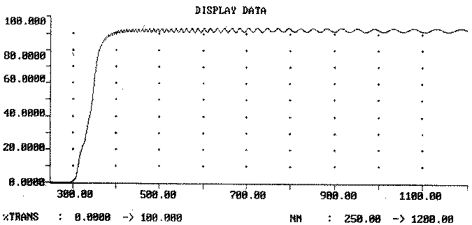
FIGURE 1: Example of spectrophotometer trace of a transparent, thin film sample.
By determining the wavelengths at maxima and minima, the product of n*d
can be determined. However, neither n nor d can be determined independently.
This is a major drawback to this method because either n or d must be
known. In semiconductor work, as
in this work, it is n that is usually assumed from literature or other
experimentation. However, the
value of n can vary due to the nature of the manufacture of the film.
This not only can lead to significant errors in d but also neglects
vital information to be gleamed from the value of n.
(For example, a lower than expected value of n may indicate a porous
film.) Both n and d could be evaluated from several maxima (and/or
minima) if the dispersive equation for the index of refraction of the film is
known to be of a definite form. However,
dispersive equation may also vary with the quality of the film.
I.2
Adaption to Reflectometer:
In order to determine the n and d values for transparent films on top
of a reflecting (non-transmitting) surface, a special adaptive fixture was
designed and built for the Cary 5 Spectrophotometer, as shown in Figure 2.
The fixture reflects the beam of light on a front surface (probably
silver) mirror up to the sample. The
light strikes the sample at an incidence angle of 30o.
Then the light is reflected on a second front surface mirror to the
detector. The fixture was
meticulously machined to assure precise angles.
The fixture was designed and produced to hold the sample parallel to
sample holder and the mirrors set, at high tolerance, 30o to the
sample holder.
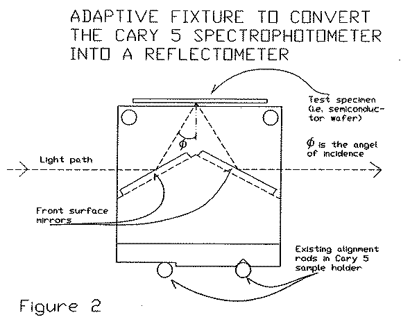
FIGURE 2:
Adaptive fixture to convert the Cary
5 Spectrophotometer into a reflectometer.
The concerns with this adaptation include:
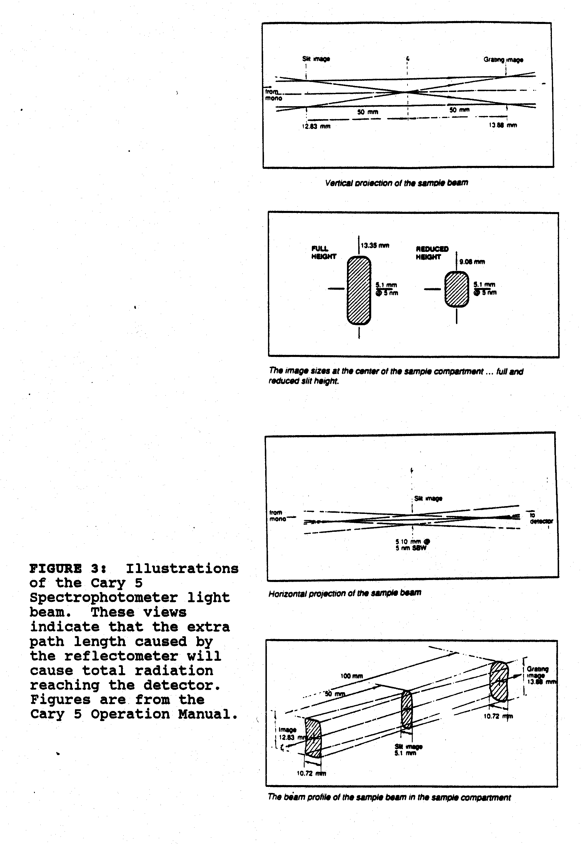
the fact that the light beam diverges (as shown in Figure 3) and is not
designed to travel the extra distance this fixture imposes, and the fact that
reflection on the two mirrors alter the nature of light.
These concerns are alleviated by the fact that data taken in reference
to a primary baseline trace. To
do a baseline measurement at the proper wavelength range, the fixture is
placed on the sample holder and a "bare" substrate is placed on the
fixture. The reflected intensity
of subsequent sample traces is recorded as the percentage of the intensity
which reached the detector when the baseline was taken.
Therefore, abnormalities caused by the fixture will be factored out.
However, one factor unaccounted for is the fact that there will be a
native oxide on the substrate used for the baseline.
However, with silicon for example, the native oxide (SiO2)
will be so thin that it will not cause gross variations.
I.3
Sample Preparation:
The author was fortunate to be granted access to the
cleanroom, to be gifted with seven 3" diameter silicon wafers, and
most notably, to receive the assistance of David Price.
All eight wafers were given an RCA clean to remove ionic and organic
contaminants as well as the native oxides.
(The description of the RCA clean procedure is included in the
Appendix.)
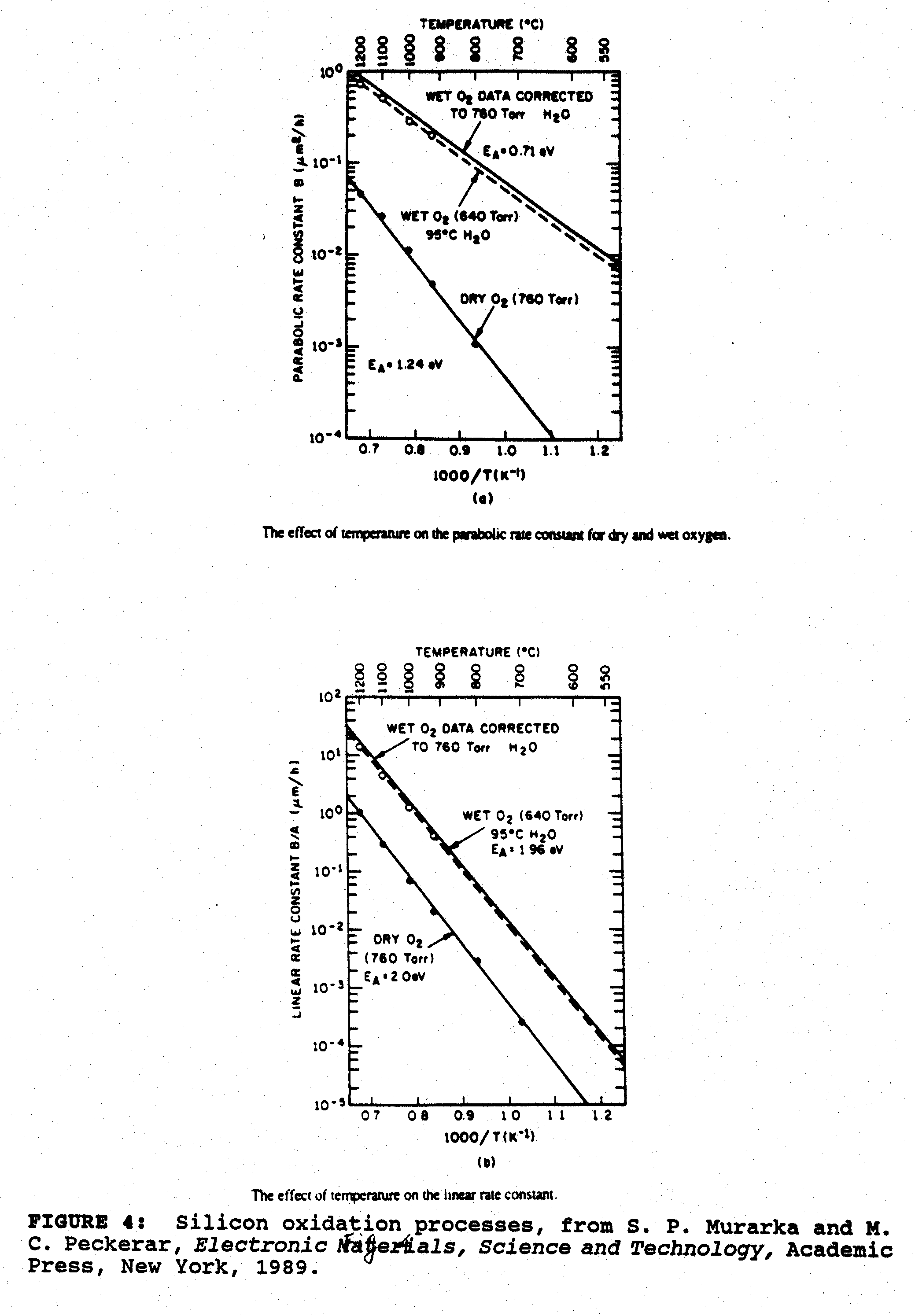
Five of the wafers were wet oxidized.
This involves placing the cleaned wafers into a furnace.
The furnace seals the wafers in a fused silica chamber heated by
elements in its wall. Oxygen and
hydrogen are introduced into the chamber at high pressure, and release heat
while turning into steam. The
steam diffuses into the silicon at a much faster rate than oxygen does, due to
ability of hydrogen to diffuse into silicon rapidly.
Therefore, wet oxidation (with steam) is used when thick oxides are
required. However, the oxide
produced is generally more porous and of lesser quality than oxide produced by
dry oxidation (no steam). Figure
4 shows the rates versus temperature for wet and dry oxidation.
Hydrogen and oxygen are introduced in a ratio of 2 : 1 and produce the
following chemical reaction with the silicon:
Si +
H2O �
SiO2 +
2H2
The parameters for the oxidation were designed to produce an oxide
thickness of one micron. The parameters include:
Ramp up: 20 minutes
Preanneal: 20
minutes
Oxidation: 17
minutes (Steam at 1,000 oC)
Postanneal: 40 minutes
Ramp Down: 40 minutes
Silicon nitride, which is typically used as a high temperature mask,
was deposited on one wafer (after RCA clean).
The nitride was deposited by chemical vapor deposition at a temperature
of 800 oC and a NH3 flow-rate of 120 liters/minutes.
The nitride was deposited for five minutes.
After the RCA clean, wax was applied to the five wafers which were
oxidized and to the wafer which was deposited with nitride.
The concept was that the wax prevents oxidation or nitride deposit.
Therefore, after these two procedures, the wax was removed (by hot
trichloroethylene) to reveal "bare" silicon surfaces.
Then a machine called a Dektak, which is basically a profilometer, uses
a mechanical stylus to slide along the "bare" silicon surface into
the surface covered with the oxide or the nitride.
The machine measures the vertical displacement of the stylus when this
occurs. This measurement is inaccurate, but it ball-parks the
thickness, which is useful because the ellipsometer returns several possible
thickness values, equally and significantly separated.
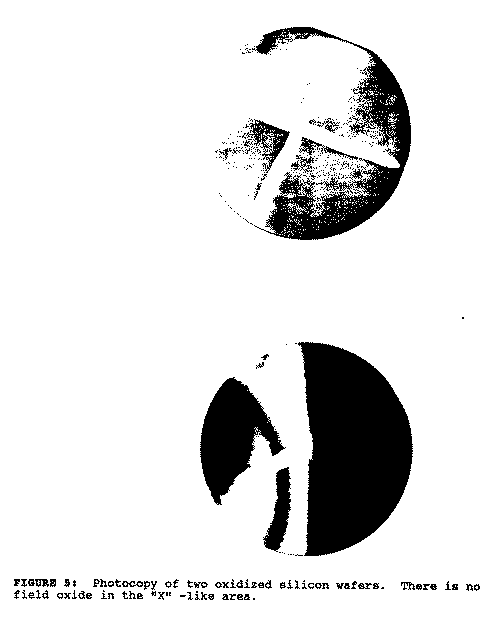
The above procedure has been described because during assistance in the
cleanroom, the wax was applied in typical manner, which was inappropriate for
this work. A thin "X" was made with the wax over the
entire wafer, as shown in Figure 5. At
first it was thought that this unfortunate action was terminal because there
was no way to position the wafer on the fixture and totally avoid radiation of
the "X" region by the spectrophotometer beam. However, not wanting to abuse the generosity of the cleanroom
personnel, it was considered that any light incident on the "X"
region the same as the baseline measurement made on a "bare" silicon
wafer. Therefore, the affect of
this region will only be seen in the maximum and minimum amplitude values, but
will not affect the wavelength values for the maxima and minima, most
important for Objective 1. This
concern will be discussed further in Objective 3.
I.4
Experimental Data Curves:
The wafer which was not coated was placed on the fixture and a baseline
trace was made, ranging from 200 to 1,000 nm.
This is shown in Figure 6. Then
the oxidized wafer was traced. The
trace is shown in Figure 7 and the test of the nitride-coated wafer is shown
in Figure 8. Before delving into calculations and manipulations of the
data, a "big picture" view of the data can be obtained by
theoretical curves for the same physical conditions.
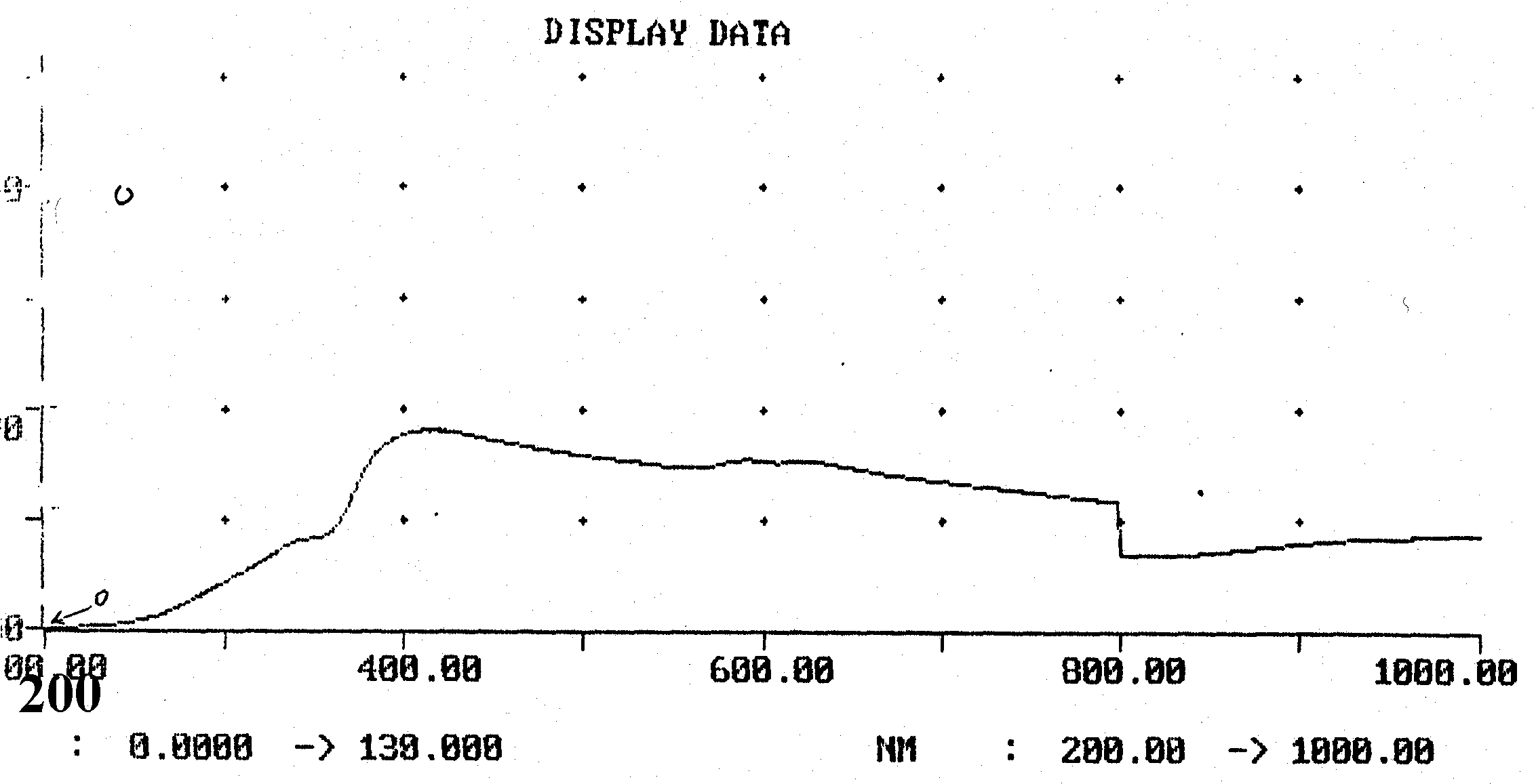
FIGURE 6:
A baseline
spectrophotometer trace. A
"bare" silicon wafer was placed on the reflectometry adaptor and this
reference trace was made.
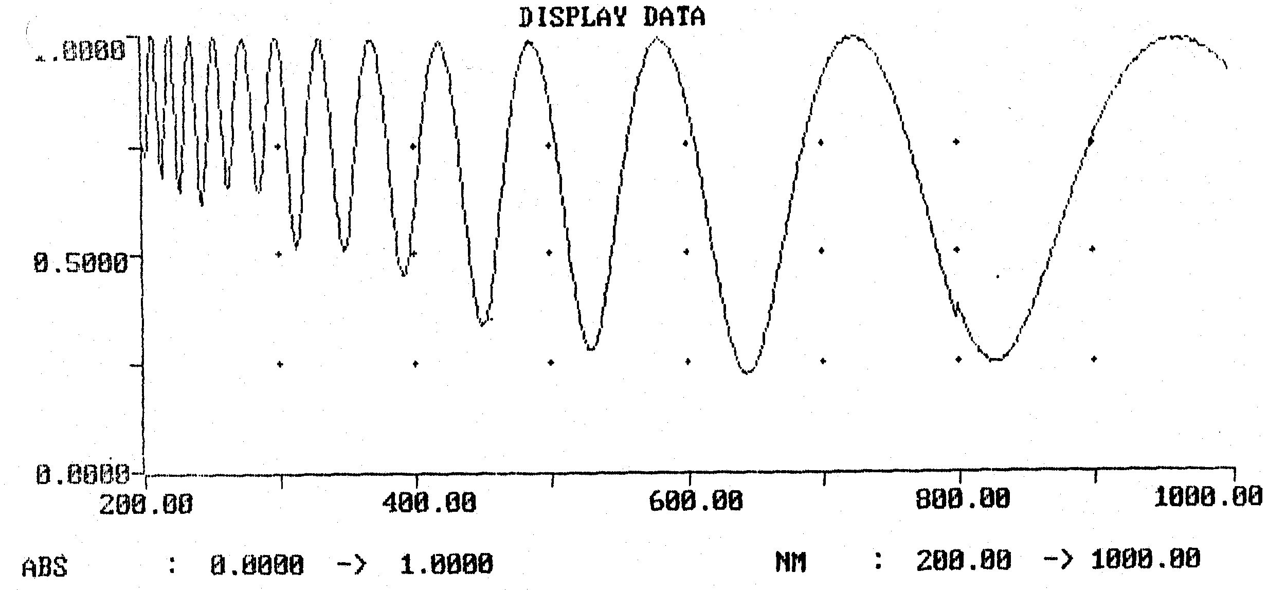
FIGURE 7:
Spectrophotometry trace of
reflection from an oxidized silicon wafer.
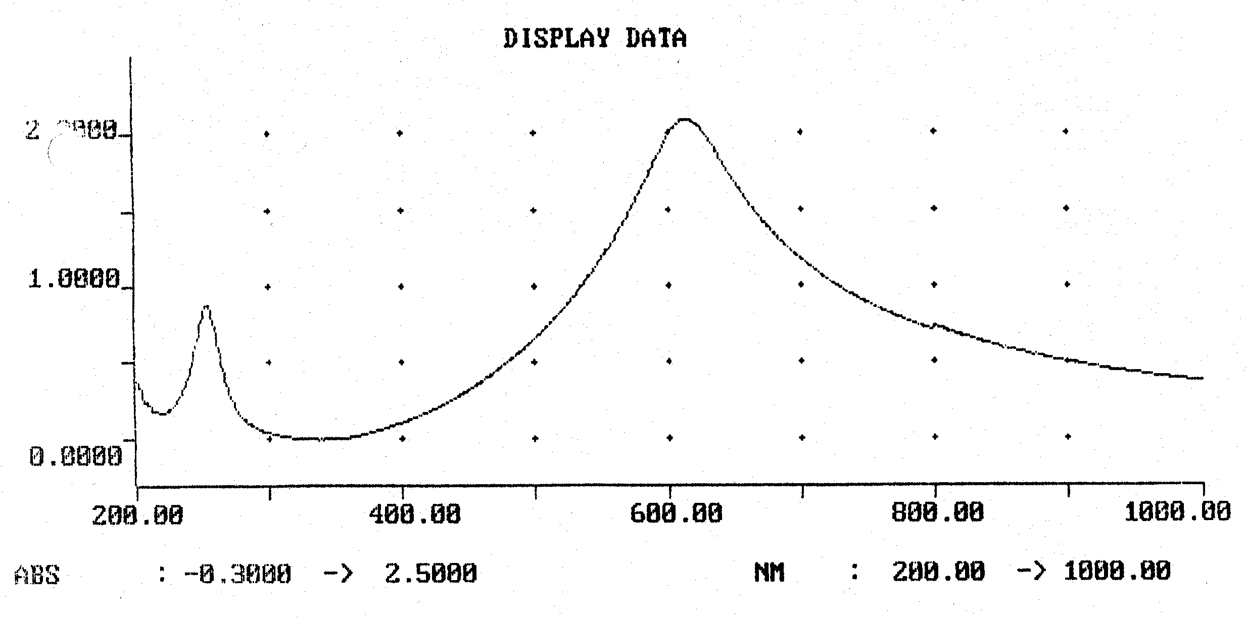
FIGURE 8:
Spectrophotometry trace of
reflection from a nitride coated silicon wafer.
I.5
Theoretical Amplitude Curves:
"Mathcad" software [2], was used to plot the theoretical
curves. The reflected amplitudes
of radiation with electric field oscillations perpendicular and parallel to
the incidence plane (Rs and Rp) were calculated via a
formula which appeared as follows:
|
|
where r's
is the reflection (of perpendicularly polarized light) from the air to
dielectric interface, r''s is the reflection from the
dielectric-metal interface, and xs is the phase change caused by
the optical path length travelled into and out of the film plus the phase
change caused by the reflection from the metal surface δs:
|
|
Note r's
and r'p, r''s and r''p, δs
and δp, and Rs and Rp, are different for
a non-zero angle of incidence. Therefore,
another major difference between this type of reflection measurements and
typical transmission spectrophotometry is the difference in the traces of
polarization components.
The thickness and index of refraction of the dielectric films were
determined, for these theoretical plots, from ellipsometry measurements (to be
discussed in the next chapter). The
cleanroom ellipsometer uses a beam laser with a wavelength of 623.8 nm.
Therefore, the value of n determined by ellipsometry is only good for
that wavelength. Since the values
of n as a function of λ are required across the range of λ used in
theoretical calculations, the Cauchy dispersion equation was assumed:
|
|
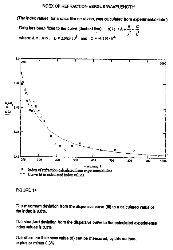
where A, B, and C are constants. These constants were approximately determined, by using the index value from ellipsometry (n632.8) and the indices at various wavelengths given in Table I for vitreous silica [3]. (The same was done for the nitride so that only the value of A differs from nitride and silica input.)
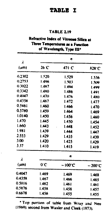
TABLE I: Index of refraction values for vitreous silica. This data was used, along with ellipsometry data, to generate constants for the Cauchy dispersion equation. (A = 1.416; B = 4,000; C = 1.533 * 107) Table taken from N. P. Bansal and R. H. Doremus, Handbook of Glass Properties, Academic Press, New York, 1986.
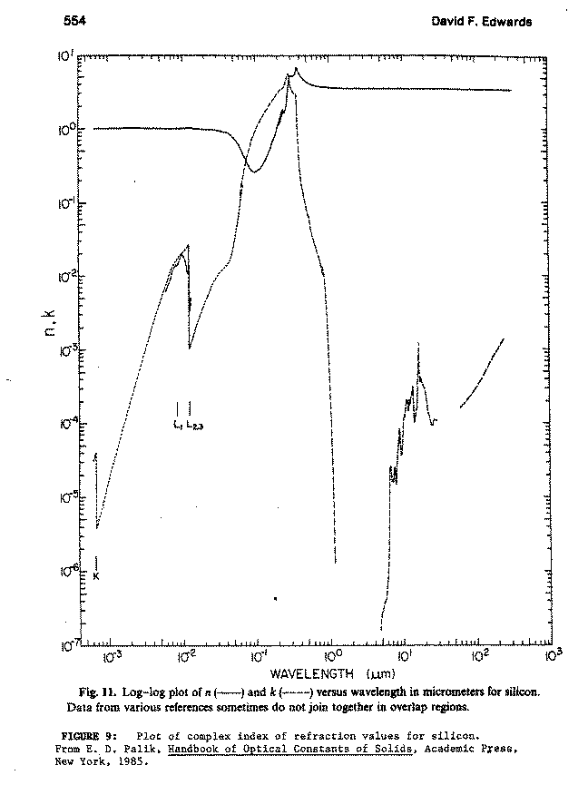
Other data required for generation of theoretical curves is the complex
index of refraction for silicon (= ns + ks*i).
Both the real and imaginary (ns and ks) parts of the index vary greatly
over the wavelength range used, as illustrated by the plot of ns and ks versus
λ shown in Figure 9. The
data used for complex index was obtained from Aspnes and Theeten [4,5] and is
shown in Table II.
The mistake was made of entering complex index values at intervals of
only 1 nm and the software limited the quantity of inputs.
Therefore, theoretical calculations are only made for λ = 200 to
799 nm by 1 and not λ from 200 to 1,000 nm as in the experimental work.
However, the 200 to 799 nm range is broad enough to yield understanding
of the theory. Lastly, the
complex index of refraction is slightly dependent on angle of incidence, but
test calculation showed variations of only tenths of a percent, thus no
attempt is made to correct for the different angles of incidence in this
study.
The Mathcad work is shown here.
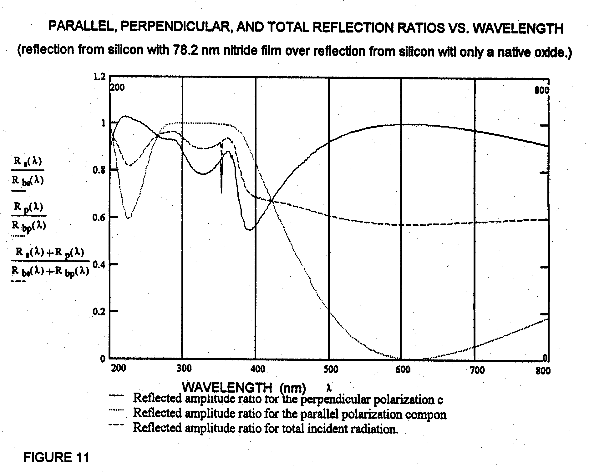
Figures 10a and 11 show three theoretical curves
plotted on the Y-axis: Rs/Rbs
is the ratio of the amplitude of the perpendicular reflected component from
the film covered substrate over the amplitude of perpendicular reflected
component which would be reflected from the bare substrate.
Therefore, Rbs is a theoretical baseline for the
perpendicular component. Similarly,
Rp/Rbp is plotted for the parallel components.
Finally,
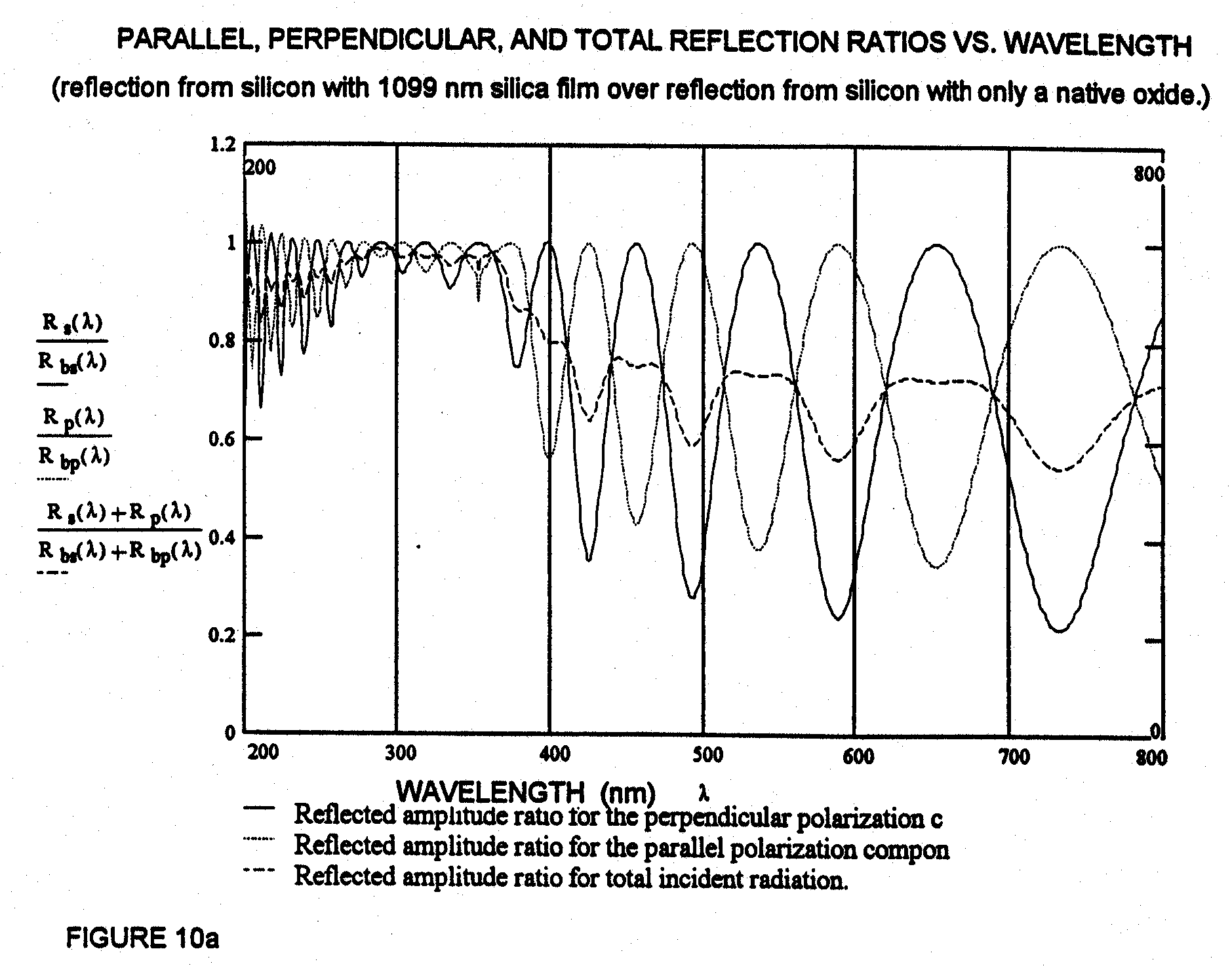
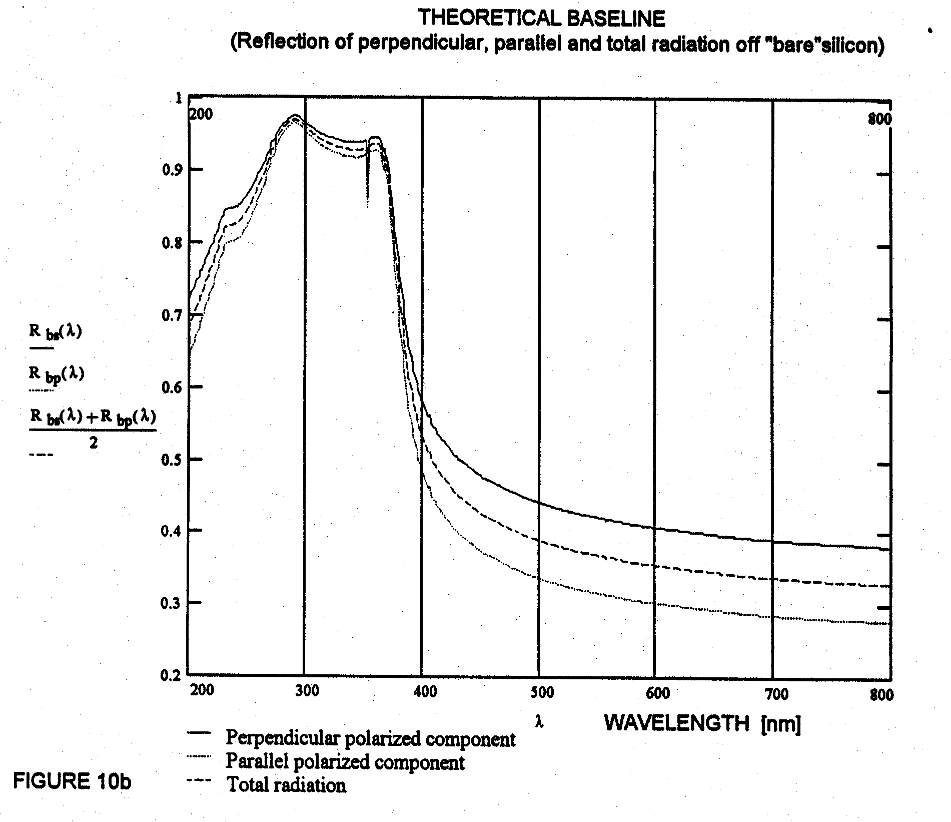
The first thing that one notices is that the sinusoidal nature of the
theoretical curves for the two polarization components matches the sinusoidal
nature of the experimental curve. But
when the two component curves are averaged to determine the total reflected
amplitude ratio, the curve cannot be considered to be sinusoidal.
It would seem that the experimental curve would be predicted by the
averaged theoretical curve, because no polarizer was purposely placed in the
system. However, this is clearly
not the case. Therefore, the Cary
5's optical elements (slits, diffraction gratings, etc.) must cause
significant polarization of the light beam.
It is noticed that the maxima and minima of the experimental curve
(Figure 7) match the maxima and minima of the amplitude curve for the parallel
polarization component exactly. This
indicates first that accurate n*d values will be determinable from the
experimental data. Secondly, it
indicates that the perpendicular polarization component has been significantly
reduced in the optical system. This
is easily proven by placing a polarizer in the system and performing baseline
traces (this test has not been performed at this time).
The second difference is seen as the sharp reduction in oscillation
amplitude for λ's below about 370 nm in the theoretical curve.
The experimental curve (Figure 7) retains significant oscillation
amplitudes in that range. The
reason for this is easily seen by comparing the experimental baseline (Figure
6) to the theoretical baseline (Figure 10b).
The experimental reflection off silicon decreases sharply for λ's
below 370 nm, while the theoretical reflection increases greatly below 370 nm.
Ignoring the native oxide, the reflection off the silicon is only
dependent upon the complex index of refraction of silicon.
This indicates how dramatically the complex index can changes in this
wavelength range, especially if the silicon is doped differently.
The silicon used by Aspnes and Theeten [4] had a resistivity of 26
Ω cm. The resistivity of the
wafers used in this study was not determined, but could be determined in the
future.