
THIN FILM ANALYSIS USING
SPECTROMETRY AND ELLIPSOMETRY
OBJECTIVE 2:
II.1 Ellipsometry:
Ellipsometry involves illuminating a sample with an elliptically
polarized light source and analyzing the reflected beam with a polarizer and a
detector. Ellipsometry can
determine the complex indices of refraction or indices and thicknesses of
single or multiple film layers. Ellipsometry
is typically used in the semiconductor industry to analyze thin films, in the
optics industry to measure the reflectivity of mirrors, and elsewhere to
analyze the properties of thin surface films.
Schematics of key ellipsometer elements is shown in Figure 15. A monochromatic light source is linearly polarized by a plane
polarizer and traverses a compensator which causes elliptical polarization.
The elliptically polarized light then strikes a sample at an angle of
incidence between 60o and 80o.
The resulting reflected wave is sent through another plane polarizer,
which is aptly called an analyzer, before entering a detector.
The first polarizer, the compensator and the analyzer can all rotate in
order to make measurements. Usually
however, the compensator is held fixed and the polarizer and analyzer are
rotated into positions which cause a null at the detector.
A null is caused when the reflected wave is linearly (or plane)
polarized and the analyzer aligned with the angle of polarization of the
reflected wave. Therefore, both
the polarizer and the analyzer have to rotate to particular angles to produce
a null. Equipment which use this
technique are called nulling ellipsometers.
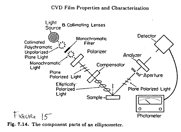
FIGURE 15: The component parts of an ellipsometer.
The two azimuth angles of the polarizer and the analyzer (P and A)
required to produce a null, can be measured with high resolution and accuracy
with this technique. It
eliminates effects caused by variation in incident beam intensity or detector
sensitivity. The polarizer and
analyzer angles needed to produce a null (P and A) are immediately converted
into theoretically defined angles: ψ
and Δ, which will be described in the next section.
The AutoEL-II, used in the cleanroom, is a nulling ellipsometer.
It uses a laser (λ = 632.8 nm) at an incident angle of 70o.
Illustrations of the AutoEL-II are shown in Figure 16 and 17, and its
specifications are described in Table IV.
Using this equipment is simple. A
wafer is placed on the sample stage. An
autocollimator microscope allows the operator to adjust the stage so that the
wafer surface is level and at the proper height.
Adjustments for level were performed prior to each measurement.
After a measurement, the AutoEL-II returns values of ψ and Δ.
These values are then entered into a PC-run program, which will
calculate the desired property values. A
list of programs available from Rudolph Research is shown in Table V.
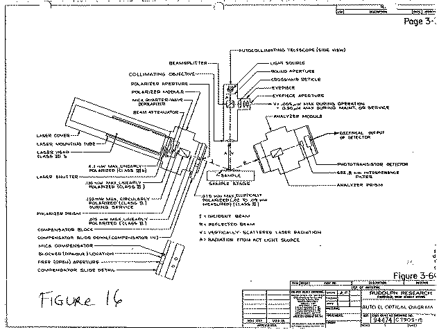
FIGURE 16: Auto El Optical Diagram.
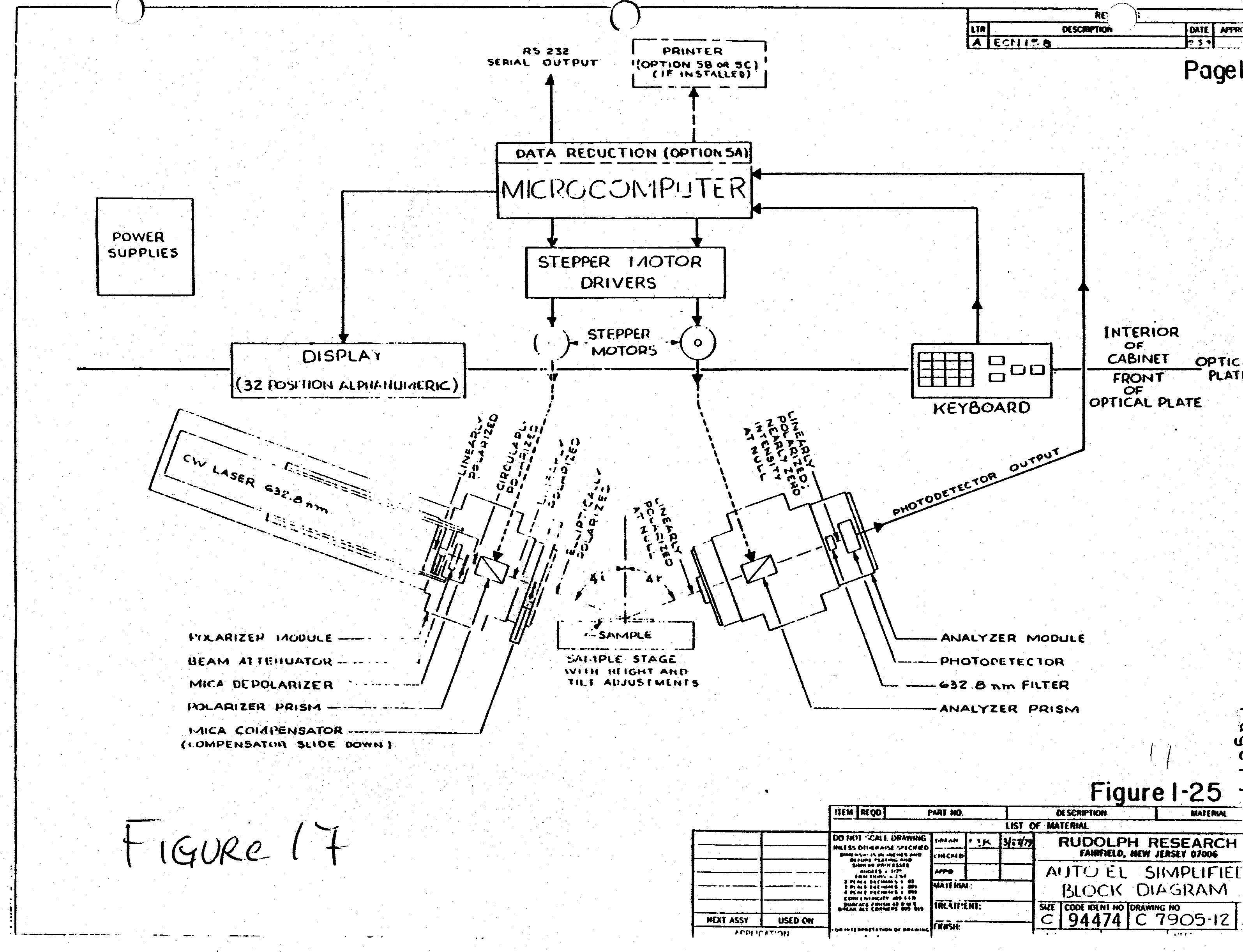
FIGURE 17: Auto El Simplified Block Diagram.
II.2 Ellipsometry Theory:
The reflectivity, ρ, is the ratio of the parallel and
perpendicular radiation reflected from a surface:
|
|
so:
|
|
where rp and rs
are the amplitudes of the reflected wave parallel and perpendicular to the
plane of incidence, δp and δs are the phase
changes between the incident and reflected waves in the parallel and
perpendicular polarization directions, respectively.
Since rp, rs, δp, and δs
are related to properties of a surface, such as complex indices and film
thickness, the values of ψ and Δ can be used to determine such
properties. The formulas derived
to evaluate properties from ψ and Δ are complicated and usually
require computer iteration to evaluate.
ψ and Δ are functions of the following variables: the angle of incidence (φ), the wavelength of incident
light (λ), the ambient index of refraction (n0), the complex
index of refraction of the substrate (or metal) (ns + i*ks), the complex
indices of refraction for each thin film (ni + i*ki),
and the thicknesses of each thin film layer (di). (Note: for
transparent thin films, ksi is assumed to be zero and the indices
real.) For a particular
ellipsometer set-up the pair of ψ and Δ values returned can be used
to determine only two of the variables above, all others must be known.
The pairs of variables typically chosen are the real and imaginary
index parts of a bare substrate or the thickness and index of the upper-most
thin film layer. Other pairs are
much harder, mathematically, to determine.
If the determination of more than two variables is required or if the
two variables chosen cannot be determined accurately (for reasons described
later), then (an) additional set-up(s) will have to be used to generate (an)
additional pair(s). This can be
done by changing the angle of incidence, the wavelength, or the index of
refraction of the ambient environment. If
the angle of incidence is changed, the new angle must be located or determined
with high accuracy. An error of
even 0.1o will cause unacceptable calculations.
Errors in angle of incidence is generally assured no greater than 0.02o.
Changing the wavelength can be easier with proper equipment.
The ambient index of refraction can be changed using a special chamber
to submerge the sample in a liquid. The
chamber is designed to allow the light beam to enter and exit the chamber at
normal incidence (it is probably also designed to allow for proper alignment
of the sample). Sometimes the
liquid used as the ambient can have an index matching the upper-most film,
thereby eliminating the influence of the that film from the calculations.
As mentioned before and shown in Equation 9 for ρ, ψ and
Δ can be related to surface properties.
Often this is done by separating a complex equation into real and
imaginary part, resulting in two equations.
These equations can be solved by iteration or graphically.
Figure 18 shows a plot of a series of ψ vs. Δ curves for
graphical analysis. Each curve
has a different constant value of n. Positions
along a single curve, determines values of δ, represented by the tick
marks and numbers (0 to 180o).
δ is represented by the following equation:
|
|
Once δ is determined from the
plot, d can calculated, using the value of nf from the curve.
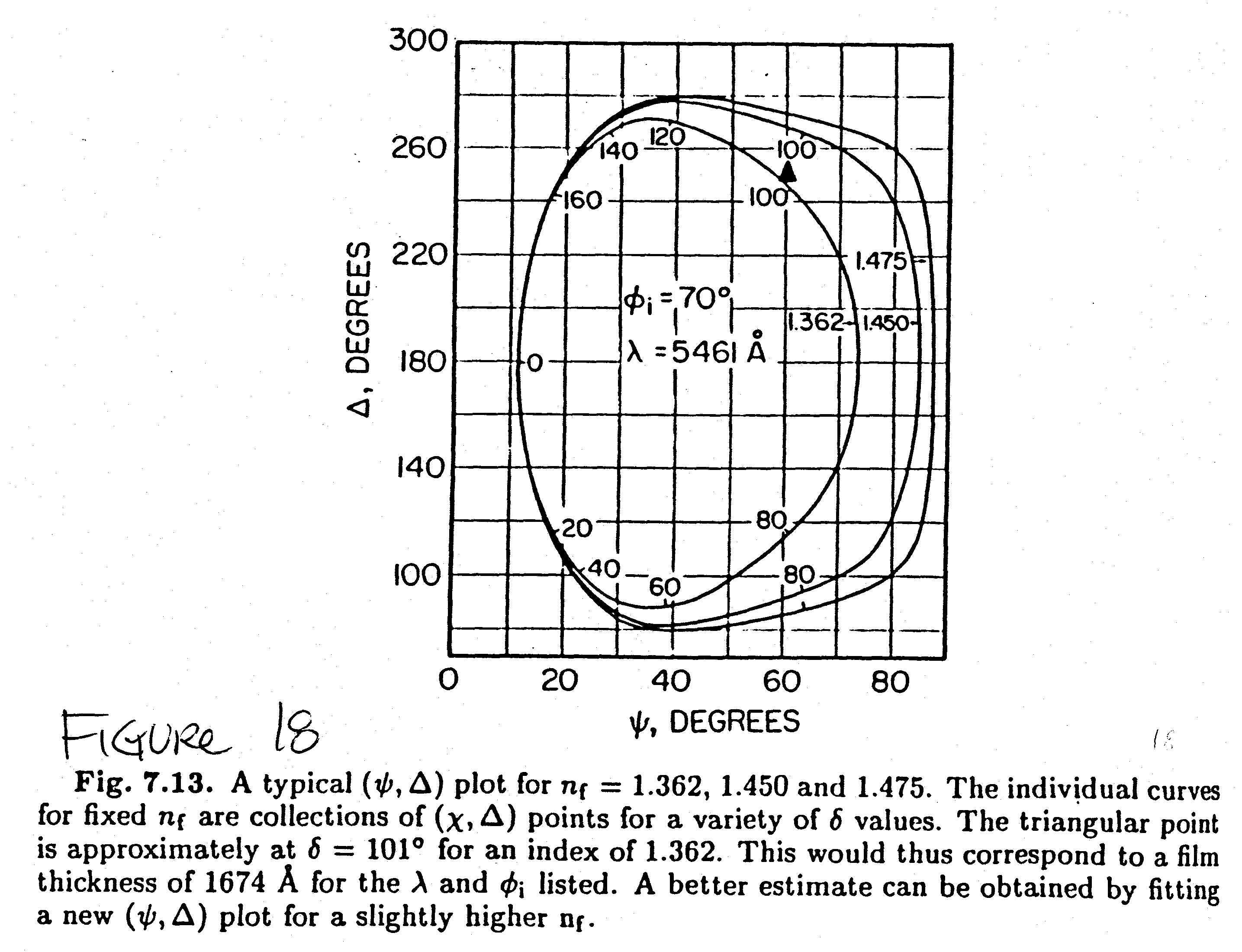
It can be seen from Figure 18 that there are certain values of δ
(from about 0 to 40 and 140 to 180) where n cannot be determined with
confidence. This has to do with
the fact that when the path length through a film is equal to a whole number
of wavelengths the ellipsometer data is the same as if there where no film at
all. Therefore, any particular
sample could potentially have properties which yield ellipsometry analysis
with large errors.
II.3 NanoSpec:
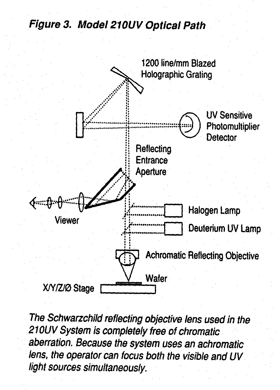
FIGURE 19: The Schwarzchild reflection objective lens used in the 210UV System is completely free of chromatic aberration. Because the system uses an achromatic lens, the operator can focus both the visible and UV light sources simultaneously.
The NanoSpec, in the cleanroom, looks like a microscope.
One places a wafer onto its stage and focuses on the wafer surface.
The NanoSpec then performs as the spectrophotometer does by reflecting
a varying monochromatic light source off of the wafer surface. A schematic of the optical elements in the NanoSpec is shown
in Figure 19. The NanoSpec is so
similar to the spectrophotometer described in the last chapter, that only the
key differences will be described here:
1. The NanoSpec analyses a
small spot (from 50 to 6.5 μm) rather the 79 mm2 (0.12 inch2)
area of the Cary 5. This allows
the NanoSpec, like the ellipsometer, to focus on a particular film on an
integrated circuit. This is very
useful, and probably more accurate than the Cary 5 if the film thickness is
varying.
2. The NanoSpec is
designed to be linked to a computer and many programs are available to
evaluate various properties. This
makes the NanoSpec extremely powerful. It
can evaluate numerous film and film combinations.
It can analyze impurities, by determining the absorption
characteristics of transparent films. This
ability is not due to the NanoSpec having better hardware than the Cary 5, but
the Cary 5 apparently does not have software to generate such information, and
certainly have not developed the software for specially adapted reflectometry
fixture presented in the last chapter.
The software for the NanoSpec is also advanced.
For example, Figure 20 shows how the NanoSpec determines thin film
thicknesses--by separating out shapes of the spectrum-generated curves, rather
than looking maxima or minima as was done in the last chapter.
The NanoSpec stresses the use of ultraviolet light for very thin film
(less than 10 nm) and for causing certain
multi-film conditions to be reduced to a single film analysis because
the polysilicon is opaque in the ultraviolet.
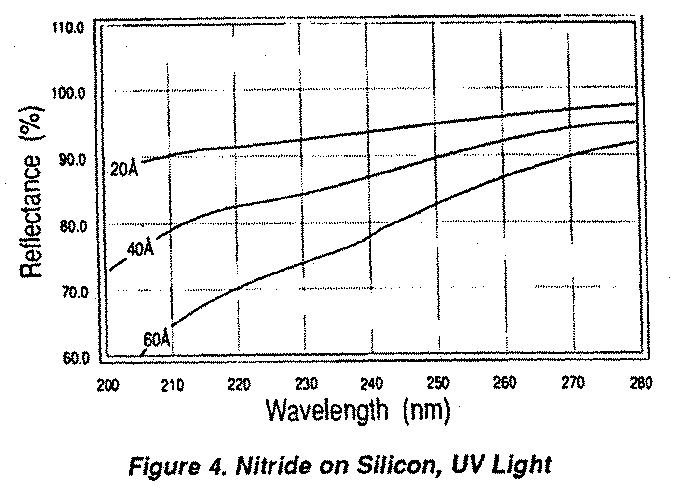
FIGURE 20: Reflectance versus Wavelength for Nitride on Silicon with UV light.
3. While the fixture
designed for the Cary 5 has a precise incidence angle of 30o, the
NanoSpec does not list a value for incidence angle.
Furthermore, observing the schematic in Figure 19, shows that the
incident light has been focused onto a sample by a reflecting lens.
This indicates that the angle of incidence may have a range associated
with it and also that this range will change when the magnification (or spot
size) is changed (a NanoSpec capability).
It is unknown how the NanoSpec programming deals with this.
4. The NanoSpec has a
wavelength range of 200 to 900 nm, this is a wide enough range for the type of
measurements required in the semiconductor industry and a wider range than
many similar pieces of equipment. However,
the Cary 5 has a wider wavelength range of 175 to 3300 nanometers.
5. The NanoSpec scans quicker than the Cary 5, which is even slower
because it has to change filters at 800 nanometers.
The NanoSpec sends all radiation from two light sources on to the
sample and scans monochromatic frequencies before reaching the detector.
Where the Cary 5 separates the light to be monochromatic before
contacting the sample.
II.4 Comparison of Data:
Data was taken by the ellipsometer and the NanoSpec at several points
on each wafer, while the Cary 5 spectrophotometer took data at only one large
area per wafer, due to the time the spectrophotometer took.
Twelve data points were taken by the ellipsometer and the NanoSpec on
each wafer. Figure 21 shows how
these points are identified. Each
wafer is denoted by a number (1,2,3...), each quadrant on a wafer is denoted
by a roman numeral, and the three points taken in each quadrant are denoted by
A,B or C (an example being a data point taken at 2-IV-A). This many data points were taken to indicate how the film
thickness varied over the wafer, knowledge which can be helpful in analyzing
the area that the Cary 5 set-up covers.
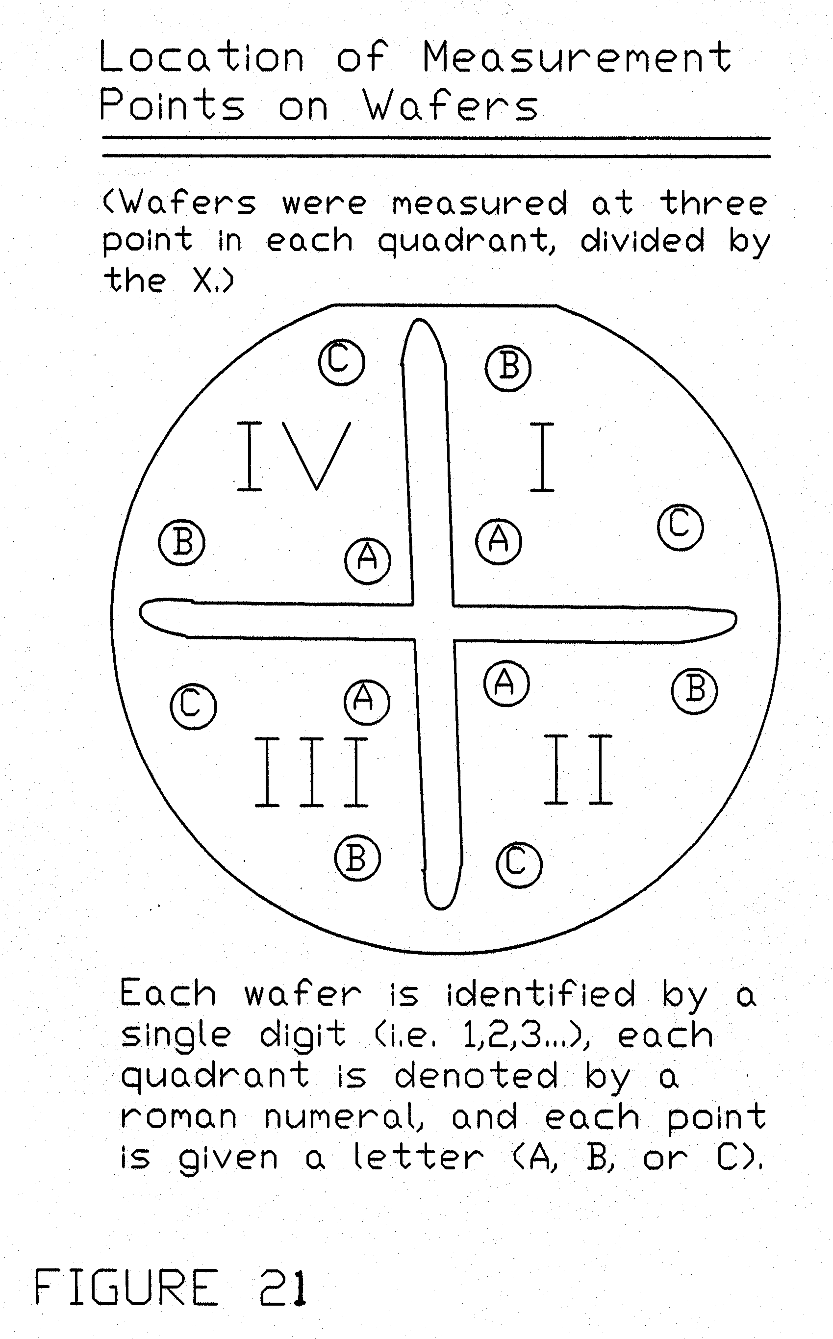
FIGURE 21: Location of Measurement Points on Wafers. (Wafers were measured at three points in each quadrant, divided by the X.) Each wafer is identified by a single digit (i.e. 1, 2, 3...) each quadrant is denoted by a roman numeral, and each point is given a letter (A, B, or C).
At each data point the ellipsometer returned a pair of ψ and
Δ values, which were typed into a near-by computer.
The computer program returned a value for the index of refraction of
the film and a series of possible values for thickness of the film. Multiple thickness values were returned because of the
cyclical nature of the phase change due to optical path difference.
Therefore, a value for the thickness was chosen by referring the value
obtain from the Dektak, a rough profilometer-like device discussed in Chapter
II.
The NanoSpec feed the information it generated directly into a
computer. The computer then
returned a value for thickness. Note
that the NanoSpec does not return several thicknesses.
This is because the NanoSpec, as well as the spectrophotometer data
obtained from the Cary 5, contain enough information to determine the order.
For example, two consecutive inflection points will determine the order
for n*d when looking at a spectrometer trace.
The NanoSpec may use a more advanced method.
One glaring flaw in the NanoSpec data was that the thickness value was
determined assuming a certain index for each type of film. For instance, the thickness for silica is determined assuming
a value of n=1.45. The operation
manual instructs an experimenter to use the following formula if the
experimenter has reason to believe that the index varies from 1.45:
|
|
where nold and Thold
are the index and the resulting thickness used and obtained by the NanoSpec
software; nnew and Thnew are the new index the
experimenter has determined and the final thickness evaluated.
The last equation suggested by NanoSpec calls the quality of its
programming math into question. The
equation and the fact that the program does not allow a new index to be input
suggests that the software does not take proper account of the dispersive
nature of n nor the influence of n on the phase change due to reflection off
the substrate.
Table VI shows the data obtained for two wafers with a silicon dioxide
film and Table VII for one wafer with a silicon nitride film.
The data used in the program which processed the ellipsometer values
are: λ = 632.8 nm, φ =
70o, and the real and imaginary values for silicon are: ns = 3.858 and ks = 0.018.
Such values were not given for by the NanoSpec.
The nnew used in Equation 12 to determine Thnew
was set at the value of n returned by the ellipsometer.
Therefore, the accuracy of the NanoSpec is linked to the accuracy of
the ellipsometer.
Table VI shows that thickness values from the NanoSpec is always 2 to 5% lower than values from the ellipsometer.
TABLE
VI
Data Points Taken on Two Silicon Dioxide Coated Wafers
|
|
|
Ellipso |
meter |
|
Nano |
Spec |
|
Data Point Number |
Delta (Δ) deg. |
Psi (ψ) deg. |
Index of film (n) |
thick- ness (d) A |
(d) A for n=1.45 |
(d) A for nellip |
|
1-IV-A |
276.20 |
31.84 |
1.426 |
10,990 |
10,520 |
10,697 |
|
1-IV-B |
276.16 |
31.84 |
1.425 |
11,000 |
10,520 |
10,705 |
|
1-IV-C |
277.24 |
33.24 |
1.429 |
10,898 |
10,520 |
10,675 |
|
1-III-A |
277.72 |
34.12 |
1.431 |
10,853 |
10,682 |
10,824 |
|
1-III-B |
278.08 |
45.12 |
1.443 |
10,483 |
10,275 |
10,325 |
|
1-III-C |
278.80 |
41.08 |
1.440 |
10,590 |
10,638 |
10,712 |
|
1-II-A |
262.96 |
22.84 |
1.409 |
11,512 |
10,868 |
11,184 |
|
1-II-B |
258.56 |
21.00 |
1.407 |
11,608 |
10,957 |
11,291 |
|
1-II-C |
249.36 |
18.12 |
1.376 |
12,200 |
11,045 |
11,639 |
|
1-I-A |
265.44 |
24.04 |
1.410 |
11,462 |
10,762 |
11,067 |
|
1-I-B |
252.44 |
19.00 |
1.387 |
11,984 |
11,061 |
11,563 |
|
1-I-C |
265.40 |
24.00 |
1.411 |
11,449 |
10,822 |
11,121 |
|
4-IV-A |
271.88 |
27.68 |
1.422 |
11,163 |
10,687 |
10,897 |
|
4-IV-B |
276.12 |
31.56 |
1.428 |
10,969 |
10,552 |
10,715 |
|
4-IV-C |
278.28 |
36.60 |
1.430 |
10,797 |
10,459 |
10,605 |
|
4-III-A |
267.92 |
25.24 |
1.417 |
11,316 |
10,769 |
11,013 |
|
4-III-B |
277.32 |
33.24 |
1.431 |
10,879 |
10,539 |
10,679 |
|
4-III-C |
256.04 |
20.12 |
1.401 |
11,737 |
10,946 |
11,329 |
|
4-II-A |
258.52 |
20.92 |
1.413 |
11,527 |
10,942 |
11,229 |
|
4-11-B |
251.56 |
18.68 |
1.392 |
11,926 |
11,004 |
11,463 |
|
4-II-C |
247.32 |
17.52 |
1.376 |
12,210 |
10,959 |
11,549 |
|
4-I-A |
264.96 |
23.80 |
1.410 |
11,474 |
10,876 |
11,184 |
|
4-I-B |
252.16 |
18.76 |
1.406 |
11,707 |
11,000 |
11,344 |
|
4-I-C |
260.76 |
21.96 |
1.403 |
11,644 |
10,796 |
11,158 |
TABLE VII
Data Points Taken on a Wafer Coated with Silicon Nitride
|
|
|
Ellipso |
meter |
|
Nano |
Spec |
|
Data Point Number |
Delta (Δ) deg. |
Psi (ψ) deg. |
Index of film (n) |
thick- ness (d) A |
(d) A for n=2.00 |
(d) A for nellip |
|
5-IV-A |
32.76 |
38.20 |
1.996 |
770 |
779 |
781 |
|
5-IV-B |
32.36 |
38.36 |
1.995 |
772 |
775 |
777 |
|
5-IV-C |
28.84 |
39.20 |
1.998 |
788 |
788 |
789 |
|
5-III-A |
30.44 |
38.84 |
1.997 |
782 |
789 |
790 |
|
5-III-B |
26.76 |
39.76 |
1.997 |
797 |
810 |
811 |
|
5-III-C |
25.64 |
39.92 |
1.999 |
800 |
808 |
808 |
|
5-II-A |
30.64 |
38.88 |
1.995 |
781 |
789 |
791 |
|
5-II-B |
32.64 |
32.64 |
1.994 |
772 |
774 |
776 |
|
5-II-C |
24.24 |
40.36 |
1.997 |
808 |
|
|
This could be due to the correction for n as described above, but then data
would be more consistently different. Another
reason why there may be difference is the fact that it was impossible to take
the ellipsometer and NanoSpec data on the exact same point, just in a close
vicinity to one another. This is
also why repeatability test were not performed.
To conduct a reasonable repeatability test one would have to move the
wafer. But there was no way to
realign test beam with the previous test point.
The wide difference between the ellipsometry and NanoSpec data calls
into question the claims that the equipment makers state.
The AutoEL-II claims the ellipsometer is accurate to "a few
angstroms" up to a film thickness of 125,000 A.
The NanoSpec makers claim accuracy of �5 A for thicknesses between 500
and 50,000 A (500 and 40,000 A for a nitride).
The error claims for the NanoSpec are evaluated as �3σ
"based upon measurement of the same spot 50 times in succession."
This may be true, but the reason why this statement is mis-leading, and
why there was no repeatability study done, is due to operator error.
Each time another data point is taken the operator has to focus or
align the sample. These are
subjective decisions of the operator and the effectiveness of the equipment
that allows the operator to do the adjustments.
Another strange fact is that, what is called "accuracy" here
has been stated as "precision" by the equipment makers.
However, they speak of "the precision" as if it were
accuracy. For instance, one does
not have to take the standard deviation of 50 points to determine precision,
one simply looks at the last digit in the read-out.
It can be seen that the silicon dioxide grown by wet oxidation varies
much more in both index and thickness, that does the deposited nitride.
This verifies that the wet oxidation process produces a low quality
(low index) and less than uniform oxide.
Table VIII compares the ellipsometer, the NanoSpec, and the Cary 5 data
determined in Chapter II. The
data points compared were taken at point 1-IV-A for the silica and at point
5-III-A for the nitride. But the
data taken on the Cary 5 was larger in area (79 mm2) which extended
into the area between points B and C, as shown in Figure 21.
Again the ellipsometer determined the value of n and that value was
used in with both the Cary 5 and the NanoSpec.
The three techniques have generated different values.
This may be somewhat due to the fact that exactly the same areas were
not used with each. However,
accuracy claims made by the AutoEL-II and
the NanoSpec have to be
challenged. Especially since the last Chapter showed that the thickness
for silica determined by the reflectometer set-up had an accuracy of �0.5%
(or �54A). The values from the
other equipment is far outside this error.
TABLE VIII
Data for Silica
and Nitride Films Determined by Three Methods
|
Film |
|
Silica |
|
|
Nitride |
|
|
Point |
|
1-IV-A |
|
|
5-III-A |
|
|
Value |
λ |
n |
(d) A |
λ |
n |
(d)
A |
|
AutoEL-II |
632.8 |
1.426 |
10,990 |
632.8 |
1.997 |
782 |
|
Cary
5 |
643 |
1.426 |
10,820 |
612 |
1.998 |
766 |
|
NanoSpec |
? |
1.426 |
10,697 |
? |
1.997 |
790 |
II.5
Comparison of Techniques:
Comparison of the three equipment set-up and techniques has already
been discussed in the course of descriptions.
However, final points will be made in the form of comparison Table IX:
TABLE IX
Comparison of the Use of the Cary 5 set-up,
the AutoEL-II, and the NanoSpec
|
# |
Equipment
and Technique |
Cary
5 |
AutoEL |
NanoSp |
|
1 |
Returns
both n and d |
No |
Yes |
No |
|
2 |
Order
determined |
Yes |
No |
Yes |
|
3 |
Dispersive
equation determined |
Yes |
No |
? |
|
4 |
Thinnest
film measurable |
? |
~700
A |
20 A |
|
5 |
Complex
index--substrate w/o film |
No |
Yes |
No |
|
6 |
Speed
at which data is taken |
Slow |
Fast |
Fast |
|
7 |
Area
of light beam for data point |
Large |
Spot |
Spot |
|
8 |
Polysilicon
made opaque by UV |
Yes |
No |
Yes |
The eight comparison points listed in Table IX will be expounded upon:
1. Returns both n and d:
This is a crucial feature which only the ellipsometer possesses.
If both are not returned the index has to be assumed to determine d and
this can cause error so large that the technology of the equipment is lost on
the effort.
2. Order Determined:
If the order is not determined then separate equipment is required to
obtain a "ball park" value. Furthermore,
if a profilometer-type device serves in this capacity, then a test wafer is
required to be included with the batch for this test.
Therefore, this test can be very expensive and time consuming in a
production scenario.
3. Dispersive Equation
Determined: The ellipsometer
determines n at only one wavelength. However, as shown in Chapter II, the spectrophotometer can
determine the dispersive nature of n. The
equation can be useful for predicting n at other wavelengths.
4. Thinnest film
measurable: As devices become
smaller and faster, thinner films are required. Currently, 16 megabit memory chips require oxide film
thicknesses of 100 A or less. Such
thin films cannot be measured by the ellipsometer, unless its Helium-Neon
laser is replaced with a laser with an ultra-violet wavelength.
The AutoEl-II manual claims that it is able to measure very thin films,
but this is doubtful. If Equation 11 for δ is considered along with Figure 18,
it can be seen that for δ to be above about 40o, d should be
above about 700 A (for n=1.426). Below
d = 700 A, the value of n rapidly decreases in accuracy.
Again it should be noted that the ellisometer may return inaccurate
values at any thickness range.
5. Complex index of a
substrate without a film: The
ellipsometer can determine the complex index of a bare substrate.
Not only can this have importance in production, but the complex index
values are required for the determination of transparent film properties by
all three methods. Chapter II
showed that more attention should be given to the determination of the complex
index of silicon, especially in the ultraviolet range.
(Chapter II showed by baseline analysis a large difference between the
complex index for the experimental wafers and that from literature for
ultraviolet radiation.) This
calls into question the claims that the NanoSpec can measure films as thin as
20 A, by using the ultraviolet region. The
NanoSpec would have to be certain of the complex index to do this. No matter what, the complex index will be a source of error
if not determined for a substrate with the particular conductivity of the test
substrate.
6. Speed at which data
can be taken: The AutoEl-II
and the NanoSpec are rapid and therefore useful in a production environment.
With the Cary 5 set-up, a baseline and a sample trace must be taken,
and each takes some time.
7. Area of light beam
for data point: The AutoEL-II
and the NanoSpec, both measure over small spot sizes.
This is superior to the Cary 5's large rectangular area for three
reasons. The spot can test a
small area, as on a wafer with integrated circuits built on it, the spot can
scan over an area and determine how the film varies, and the area is not
advantageous as a averaging device because measuring an area in which the film
varies will only serve to distort the values not average them.
8. Polysilicon made
opaque by UV: It was
mentioned before, that it can be very advantageous to reduce a multi-layer
film scenario to a single film on polysilicon scenario by using ultraviolet
light for the measurement. The
ellipsometer, with its current laser does not have this capability.
Therefore, the expensive practice of using a test wafer in certain
procedures would have to be used.
II.6
Polarized Spectrophotometer:
It was mentioned at the end of Chapter II that both n and d values
could be obtained from the spectrophotometer set-up if traces were taken in
the two polarization directions. One way to obtain this result with the existing set-up would
be to design another fixture, similar to the one designed, but this one would
set on its side (turned 90o from the first). A mock example of such a plot is shown in Figure 22.
If a vertical (constant λ) line is drawn anywhere on the plot, the
line will cross the values of Rp and Rs for a particular
wavelength. This is enough to
determine ψ by:
|
|
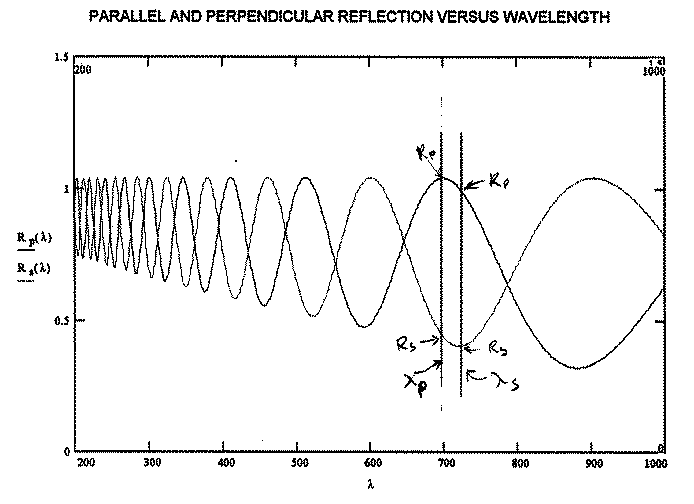
FIGURE 22: Parallel and Perpendicular Reflection versus Wavelength.
Also each
maximum or minimum for one curve is adjacent to a maximum or minimum for the
other polarized component curve, with the same value of m (the order integer).
Therefore, Δ can be evaluated by:
|
|
where λp
and λs are the wavelength at the inflection points for
parallel and perpendicular components respectively.
Since Δ is small for silicon, it can be assumed that n remains
constant from λp and λs in Equation 14.
Therefore, this system behaves as a ellipsometer by returning ψ
and Δ. But it returns a pair
of these values at several points allowing much more capabilities, such as
determining all the values in multiple films.
Furthermore, n*d values are determined at each inflection point.