
THIN
FILM ANALYSIS USING SPECTROMETRY AND ELLIPSOMETRY
OBJECTIVE 3:
III.
DOUBLE FILMS:
One of the oxidized wafers was analyzed in the ellipsometer for film
thickness and index. Then it was
coated with a photoresist, a polymer used for lithography.
The wafer secured by vacuum to a spindle and spun while the photoresist
liquid was applied. The speed of
the spindle increased afterward to increase film uniformity.
After spinning, the wafer was baked to harden the photoresist.
Then evaluation of this double film was attempted by all three methods.
III.1
NanoSpec:
The use of the NanoSpec is discussed first because it was the easiest.
The NanoSpec has a program to perform just such as analysis.
The double film wafer was just focused in the NanoSpec like any other
wafer. The program uses a value
of n = 1.64. The program returned
a thickness value of 17,400 A. Several points were taken but only this value will be given
here.
III.2
Spectrophotometry:
The experimental spectrophotometry curve for the double film wafer is
shown in Figure 25. A MathCad program was written to simulate the condition in
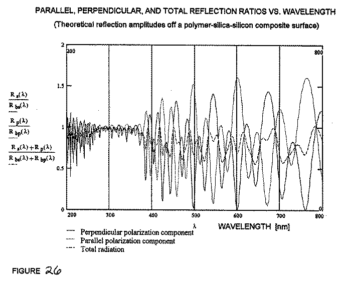
the film using, values from the NanoSpec. Figure 26 shows
the resulting plot. There
are similarities between the experimental curve and the parallel
polarization component. However,
the resemblance is not as close as with the silica covered wafer.
One reason for this may be the fact that the "X" region of
bare silicon was also coated with photoresist.
Therefore, the spectrophotometer may be observing two different
conditions to some extent.
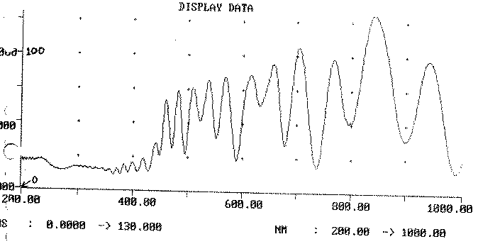
FIGURE 25:
FIGURE
26:
Parallel, Perpendicular, and Total Reflection Ratios versus
Wavelength. (Theoretical reflection amplitudes off a
polymer-silica-silicon composite surface.)
No doubt, there are mathematical methods of determining film thickness
and index from such a trace. However,
they would be too complicated to be used in this project.
Therefore, a simple method is used to determine n*d from the experimental
plot. This method uses the fact
that there will be a maximum or minimum in the plot when the optical path length
in the photoresist is equal to a whole number of wavelengths.
This is not true for the oxide layer due to the phase change that occurs
at the substrate. Fortunately, the
value of photoresist thickness was determined by the NanoSpec.
Thus, using that value it is possible to check each peak to see if it is
a peak for the photoresist. This is
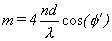
accomplished by the following equation:
 16
16
|
where, a valid
inflection point is found when m is a whole number and φ' is equal to 17.75
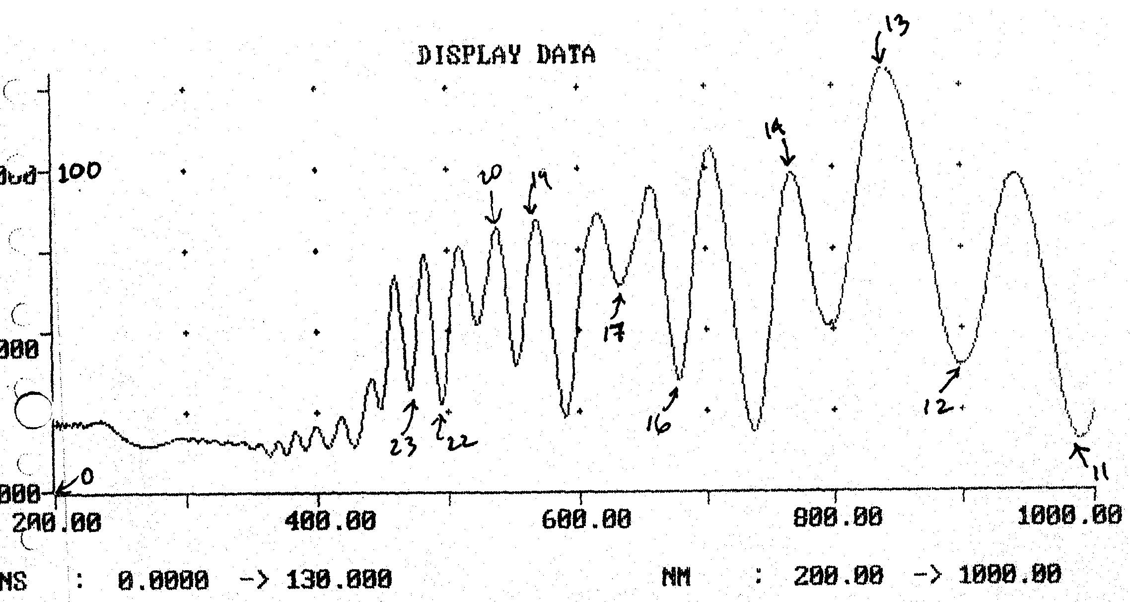
in this case. A copy of the
experimental data is shown on Figure 27, with m values written next to the valid
peaks or valleys. The data
generated from this plot is presented in Table X.
A value of n of 1.64 was used in these calculations.
FIGURE
27:
TABLE X
Data Points from a
Spectrophotometer
Trace of Double Film
on Silicon
|
m
|
λ
[nm]
|
d
[nm]
|
|
23
|
468
|
17,230
|
|
22
|
494
|
17,400
|
|
20
|
536
|
17,160
|
|
19
|
568
|
17,270
|
|
17
|
632
|
17,200
|
|
16
|
679
|
17,390
|
|
14
|
765
|
17,140
|
|
13
|
838
|
17,440
|
|
12
|
898
|
17,250
|
|
11
|
992
|
17,470
|
Table X shows widely varying values of thickness.
They are not decreasing with wavelength, as might be expected since it
was evaluated with constant n value. Therefore,
it is assumed that there is significant errors in the values.
Again this may be due to the "X" region.
III.3
Ellipsometry:
The ellipsometer is capable of determining both the n and d values for
the top film if the properties of the lower film and the substrate are known.
The values of ψ and Δ returned for the double film are ψ =
33.24 and Δ = 71.76. These
values could now be put into a computer program and the values of n and d would
be determined. However, such a
program was unavailable. Therefore,
the math to solve this problem will be presented.
Go to Abstract & Intro.
Go to Objective #1
Go to Objective # 2
Go to Objective # 4
See
our Surface Oxide Tester, which measures the film thickness' on copper in
Angstroms with the speed and user-convenience required in QC Test Labs.
Copyright � 2004 Redeeming Time
Designs Co. All rights reserved.